The Design & Verification Conference & Exhibition is the premier conference on the application of languages, tools, methodologies and standards for the design and verification of electronic systems and integrated circuits. The focus of this highly technical conference is on the practical aspects of these technologies and their use in leading-edge projects to encourage attendees to adopt similar techniques to improve their own design and verification flows.
This invite for the design contest, titled “VEGA microprocessor (RISC-V) based Design & Verification Challenge” presents unique opportunities for academic students:
1. Achieve deeper understanding of RISC-V architecture, indigenous VEGA Microprocessor and ecosystem.
2. Explore the design and verification space for better performance.
3. Implement your own hardware accelerator on industry standard FPGA in for a specified application.
4. Opportunities to interact with experts from industry and academia.
5. To win cash prizes and potential intern opportunities at leading-edge VLSI and sponsor companies
VEGA is a series of high-performance processors including India’s first indigenous 64-bit multicore RISC-V based Superscalar Out-of-order Processor, developed by C-DAC as part of the Digital India RISC-V (DIR-V) program by the Ministry of Electronics and Information Technology (MeitY), Govt. of India. These high-performance processors are based on the open-source RISCV Instruction Set Architecture with Multilevel caches, Memory Management Unit and Coherent Interconnect. Six processors are currently available in the VEGA processor family. These indigenous microprocessors employing the state-of-the-art architecture have a performance which is at par with other commercially available processors. The microprocessors are available as soft IPs and are amenable/ customizable for better performance/power targeted for various strategic/industrial/commercial applications.
The design contest will involve:
- Problem statement solution based on RTL Design, Functional verification, and implementation on an FPGA.
- Each team with maximum of 3 members should register and will be given five months with specific milestones for completion in multiple stages.
- There will be mentoring sessions at different milestones during the contest duration.
- Remote access to Genesys 2 FPGA Board and simulator/synthesizer will be provided.
- Final implementation, demonstration and evaluation on Genesys board at the venue.
Congratulations to Design Contest Stage 2A winners!
REGISTRATION PROCESS
This design contest is open only for students who are currently enrolled in educational institutions pursuing BTech/BE 2nd/3rd year, 1st year MTech/MS and PhD
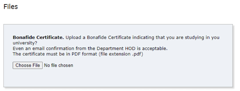
Each participant should upload a Bonafide certificate or email of their student status from the University/College by May 15, 2026
Register via the EasyChair – Register Here by February 14, 2026.
Please refer to appendix section for registration guidelines
IMPORTANT DEADLINES
January 26, 2026: Registrations for Design Contest open
February 14, 2026: Last Date for Registrations for Design Contest
February 23, 2026: Problem Statement announcement
February 24 – March 10, 2026: Stage 1 – Planning and Idea submission
March 23, 2026: Announcement of Stage 1 result
March 24 – April 27, 2026: Idea Implementation & Simulation
April 27, 2026: Final date for Stage 2 Results submission
May 11, 2026: Announcement of Stage 2 result
May 12 – June 29, 2026: Stage 3A – Hardware implementation process
June 29, 2026: Hardware Implementation Results submission
July 13, 2026: Stage 3A results
July 14, 2026 – Aug 28, 2026: Stage 3B – Hardware Implementation in FPGA
Aug 31, 2026 – Sep 1, 2026: Hardware implementation and in-person evaluation
Sept 2, 2026: Results to be announced at Conference.
STAGES
Stage-1: Planning & Idea Submission
- Your idea submission should cover
- Detailed description of the algorithm and its design feasibility along with an overall block diagram of your idea
- Benefits and value addition of your proposed solution
Stage-2: Idea Implementation & Simulation
- Simulation of the proposed application.
Stage-3: Hardware implementation
- Synthesis of the design and implementation on FPGA
- Demonstration of the application
SELECTION CRITERIA
The winners will be selected by the judges from DVCon India with weightage on complexity of the algorithm, usefulness of the application, innovation and design feasibility.
CASH AWARDS
- INR 60,000 for the Winning team
- INR 42,000 for First Runner up
- INR 30,000 for the Second Runner up
The top three winners will be given free registration to DVCon India 2026 and opportunity to demonstrate the Design Contest solution at DVCon India 2026
CONFERENCE SCHEDULE
- September 1-3, 2026 — Tutorials, Panels, Technical papers & Poster Session, Award Winners
Design Contest Chair
Seru Srinivas
Marvell
Academia Collaboration Chair
Dr. Vivek Chaturvedi
IIT Palakkad
Academia Collaboration Co-Chair
Dr. Bibhas Ghoshal
IIIT Allahabad
C-DAC Liaison
Krishnakumar Rao S
C-DAC Thiruvananthapuram
Sri Lanka Liaison Chair
Upul Ekanayaka
ACCELR
APPENDIX
Guidelines for DVCon India 2026 – Design Contest Registration
Step 1: Select the DVCon India 2026 – Design Contest Track

Step 2: Enter the Team Member Details (3 Team Member details needed)
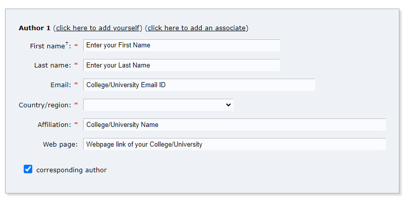
Step 3: Enter your Team name in the Title Field

Abstract: Enter “NA”
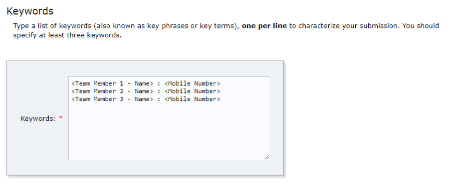
Step 4: Enter the Team Member Names and their phone numbers as indicated below.
Topics: Skip this
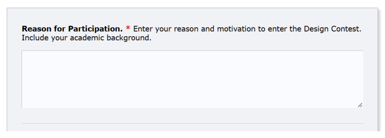
Step 5: Update your motivation for participation
Step 6: Upload the Bonafide Certificate from your college. (This can be done later)